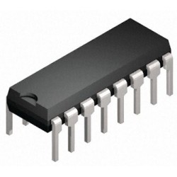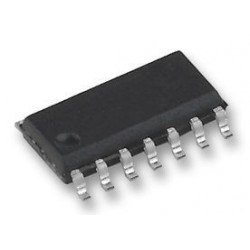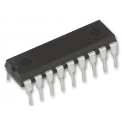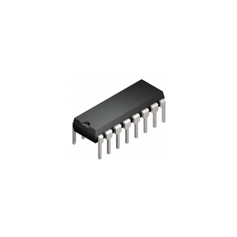


CD4027BE, 4027 Flip-Flop, Master/Slave, Complementary Output, Positive Edge, CD4027, JK, 45 ns, 24 MHz
The CD4027BE is a Single Monolithic Chip Integrated Circuit, containing two identical complementary-symmetry J-K flip-flops. Each flip-flop has provisions for individual J, K, set, reset and clock input signals. Buffered Q and Q\ signals are provided as outputs. This input-output arrangement provides for compatible operation with the RCA-CD4013B dual D-type flip-flop. The CD4027BE is useful in performing control, register and toggle functions. Logic levels present at the J and K inputs along with internal self-steering control the state of each flip-flop, changes in the flip-flop state are synchronous with the positive-going transition of the clock pulse. Set and reset functions are independent of the clock and are initiated when a high level signal is present at either the Set or Reset input.
Set-reset capability
Static flip-flop operation, retains state indefinitely with clock level either high or low
Medium speed operation - 16MHz (typical) clock toggle rate at 10V
Standardized, symmetrical output characteristics
100% tested for quiescent current at 20V
Maximum input current of 1µA at 18V over full package-temperature range, 100nA at 18V and 25°C
5, 10 and 15V parametric ratings
Get our latest news and special sales

CD4027BE, 4027 Flip-Flop, Master/Slave, Complementary Output, Positive Edge, CD4027, JK, 45 ns, 24 MHz
